
EP4CE15 + Quartus Prime 25.1 Standard + Nios V 从 0 到跑通实战记录
整理时间:2026-08-08
实测平台:Cyclone IV EP4CE15 + Quartus Prime 25.1 Standard + Nios V + Ashling RiscFree IDE
最终状态:32 KB On-Chip RAM 下 LED 流水灯成功编译、生成RAM.hex、下载 ELF,并在 RiscFree / Nios V 调试链路上跑通。
0. 最终结论先看
这次整个过程里最关键的几个结论是:
-
Quartus 25.1 Standard 的 Nios V Platform Designer 系统应先 Generate HDL,再把生成的
.qip加入 Quartus 工程;不要把.qsys当普通 HDL 源直接综合。 -
Nios V 生成的
.qip不是“模块本身”,顶层 Verilog 应实例化生成 HDL 中的niosv模块。 -
32 KB RAM 对应地址范围:
- 起始:
0x00000000 - 结束:
0x00007FFF elf2hex的-e 0x00007FFF是正确的。
- 起始:
-
.rwdata/.bss is not within region RAM的本质是程序超出 32 KB,而不是elf2hex出错。 -
删除
printf能减小程序,但本次真正让 32 KB 工程链接成功的关键是 使用 Release 构建,让 BSP 的-O2优化真正生效。 -
最终一次成功构建的报告:
- Program size:
24.91 KB - Free for stack + heap:
1260 B RAM.hex成功生成。
- Program size:
-
jtagconfig -d能看到Nios V #0并不代表 hart 一定能被 Ashling 正常调试。 -
本次
Error occurred during enumeration of RISC-V harts (no harts found)最终不是 USB-Blaster I/III 导致的。 -
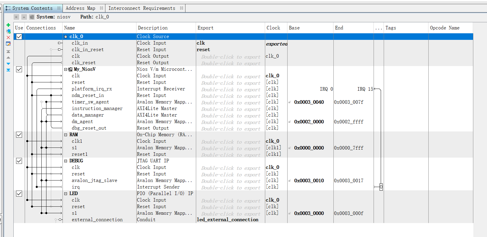
最终关键修复是 Platform Designer 中 Debug Reset 连接错误:
dbg_reset_out -> ndm_reset_in- 不要把
ndm_reset_in错接到普通 system reset dm_agent同时连接 instruction/data manager,且两边地址一致。
-
改 Platform Designer 后,已有 BSP 用:
niosv-bsp -u software/bsp/settings.bsp不要在
-u时再传--sopcinfo。 -
RiscFree 若提示旧 Debug session 未结束,先 Terminate 上一次 Ashling/GDB 会话再下载。
-
4 位 LED 若低电平点亮,可在软件输出处统一反相:
IOWR(LED_BASE, 0, (~LED_TBL[i]) & 0xF);
1. 工程结构和开发环境
本次最终使用:
- FPGA:Cyclone IV
EP4CE15 - Quartus Prime:
25.1 Standard - Platform Designer:创建 Nios V 系统
- CPU:Nios V
- On-Chip RAM:最终缩到
32 KB - PIO:4 bit LED
- JTAG UART:
DEBUG - RISC-V Debug Module:
dm_agent - IDE:Ashling RiscFree
- 软件工程:CMake +
niosv-bsp+niosv-app - Toolchain:
riscv32-unknown-elf-*
最终 BSP 中的关键地址:
| 模块 | 地址 |
|---|---|
| RAM | 0x00000000 - 0x00007FFF |
My_NiosV_dm_agent |
0x00020000 - 0x0002FFFF |
| LED | 0x00030000 - 0x0003000F |
| DEBUG / JTAG UART | 0x00030010 - 0x00030017 |
My_NiosV_timer_sw_agent |
0x00030040 - 0x0003007F |
操作过程:
首先创建一个对应板卡芯片的项目。

点击图标打开Platform Designer
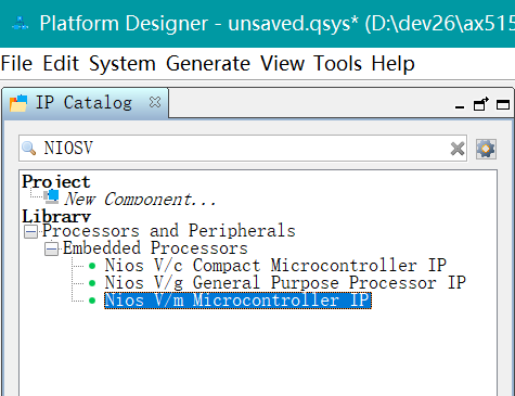
在IP Catalog搜索NiosV,双击Nios V/m Processor Intel FPGA IP以添加此IP到qsys系统,暂时保持默认参数设置不变,直接点击Finish。
用同样的方法搜索并添加On-Chip Memory (RAM or ROM) Intel FPGA IP,限于大风IV E15 较少的BRAM。Total Memory Size修改为32768(对应32K),其余参数不变。
继续搜索并添加JTAG UART Intel FPGA IP到系统,默认参数设置不变。
最后搜索添加PIO (Parallel I/O) Intel FPGA IP,Width设置为4(开发板上的LED数量),Direction设置为Output。
修改Nios V/m IP的参数设置,勾选Enable Reset from Debug Module,Reset Agent选择SRAM.s1。
右键模块可以重命名,最终连线效果:
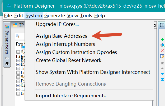
点击Platform Designer的菜单System—— Assign Base Addresses给每个模块分配地址空间。
最后点击窗口右下角的Generate HDL按钮生成qsys文件。然后把qip文件放到项目里。
再添加一个顶层模块,niosv的例化方式可以在 niosv_inst.v 里找到:
module my_first_niosv
(
    CLOCK_50,
    LEDR
);
input          CLOCK_50;
output [3:0]   LEDR;
    niosv u0 (
        .clk_clk                        (CLOCK_50),   //clk.clk
		  .reset_reset_n                  (1'b1),
        .led_external_connection_export (LEDR)  // led_external_connection.export
    );


endmodule
点击Analysis & Synthesis进行分析与综合。
分析综合完成以后,点击Quartus菜单Assignments——Pin Planner。
最后再点击Start Compilation图标编译Quartus工程,最终生成.sof文件。
软件部分:
点击电脑左下角的开始菜单打开Nios V Command Shell。
将路径切换到my_first_niosv工程文件夹路径下,然后新建software文件。
运行niosv-bsp -c -t=hal --sopcinfo=niosv.sopcinfo software/bsp/settings.bsp命令在software文件夹创建Nios V BSP。
在software文件夹路径下再创建app文件夹,并在app文件夹下创建空白led.c文件
运行niosv-app -a=software/app -b=software/bsp -s=software/app/led.c命令在app文件夹生成CMakeLists.txt文件。(后面会在RIscFree IDE 中通过“Create a New Project” wizard创建软件工程,然后通过CMakeList.txt 来把APP project 导入进去。)
打开:RiscFree IDE
workspace指向software文件夹路径。然后点击Launch启动IDE软件。
点击Create a project,在New Project窗口,选择C/C++下的C Project,点击Next以打开C Project窗口。
在C Project窗口,Project name命名为app,Location指向app所在文件夹,Project Type选择CMake driven下的Empty Project。
接下来的Select Configurations窗口保持默认设置不变,点击Finish即可。
在led.c文件里面敲入如下代码:
//#include <stdio.h>
#include "system.h"
#include "alt_types.h"
#include "altera_avalon_pio_regs.h"
/* 流水灯控制数组,高电平点亮  */
const alt_u32 LED_TBL[] = {
		 0x1,
		    0x2,
		    0x4,
		    0x8,
		    0x4,
		    0x2,
		    0x1
};
//////////////////////////////////////////////////////////
//
// function: main
// description: perform cyclically lighting the LED
// parameter: none
// return: 0
//
//////////////////////////////////////////////////////////
int main(){
  //  printf("Realize the function of cyclically lighting the LED\n");   //在console窗口打印信息
    alt_u8 i;
    volatile alt_u32 delay;
    while(1){
        for(i = 0; i<7; i++){                          //流水灯花样数组共有 7种状态
           // IOWR(LED_BASE, 0, LED_TBL[i]);          //流水灯花样显示
        	IOWR(LED_BASE, 0, (~LED_TBL[i]) & 0xF); 	//低电平点亮,取反
            delay = 0;
            while(delay < 4*500000)                       //延时大约1秒
                delay++;
        }
    }
    return 0;
}
右键项目点击属性,然后找到C/C++ Build -> Cmake4eclipse -> Manage Configurations 选择Release 点击Set Active。(不然debug下生成的固件太大放不下。)
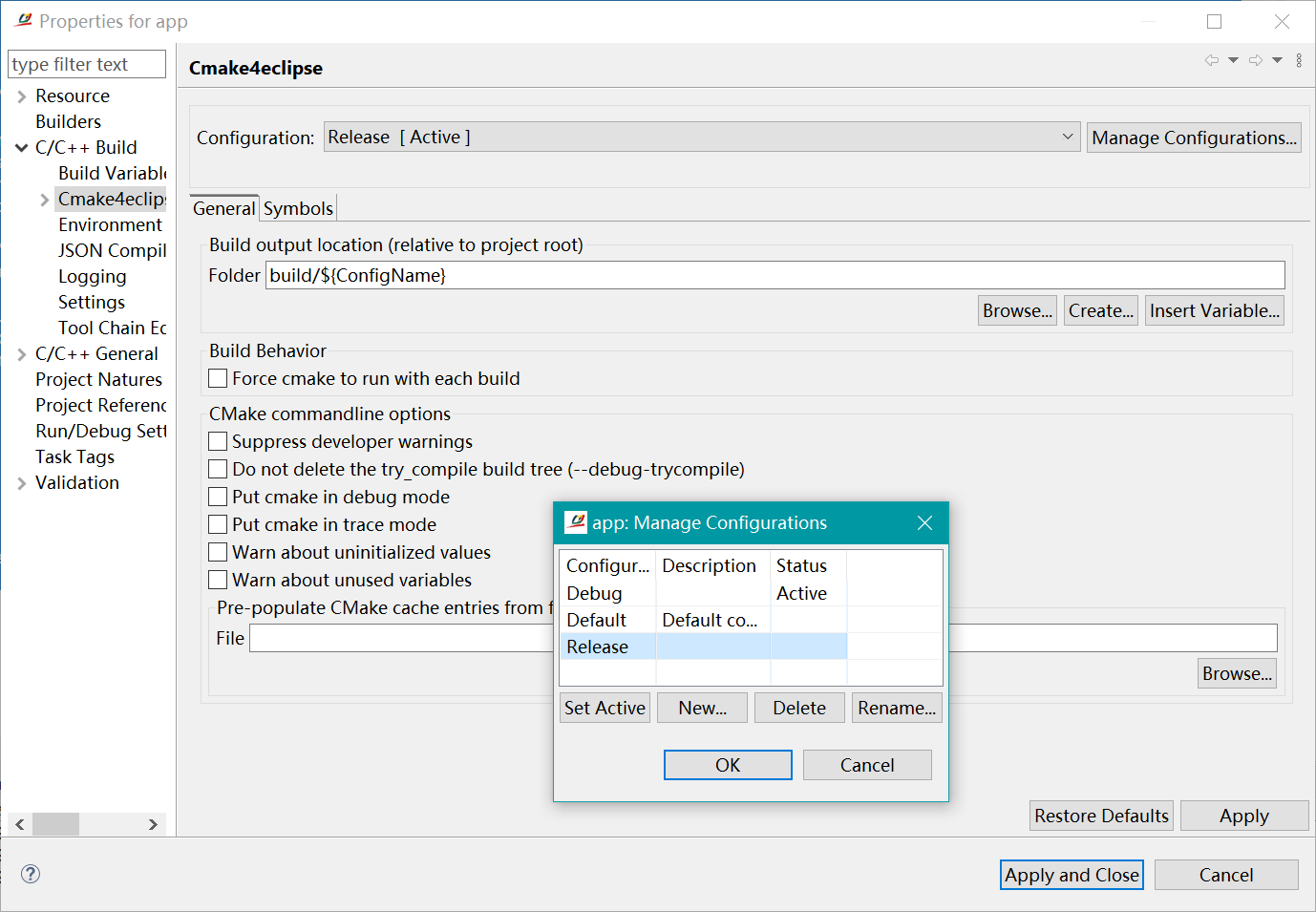
左键选中app,点击Build Project编译led.c,编译完成可以看到生成app.elf文件
下板测试:
首先在quartus里下载逻辑固件。
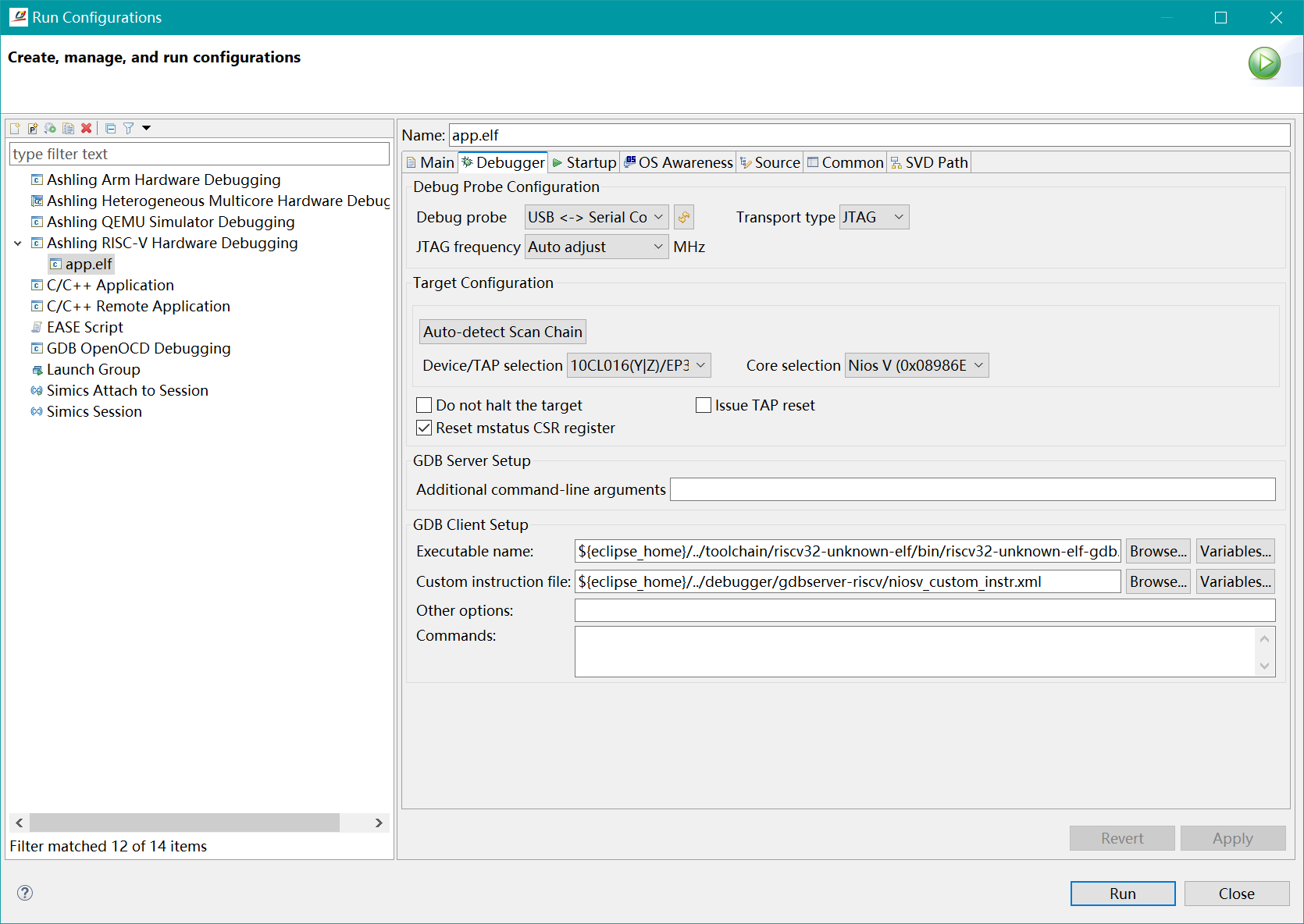
然后右键项目,配置启动方式。
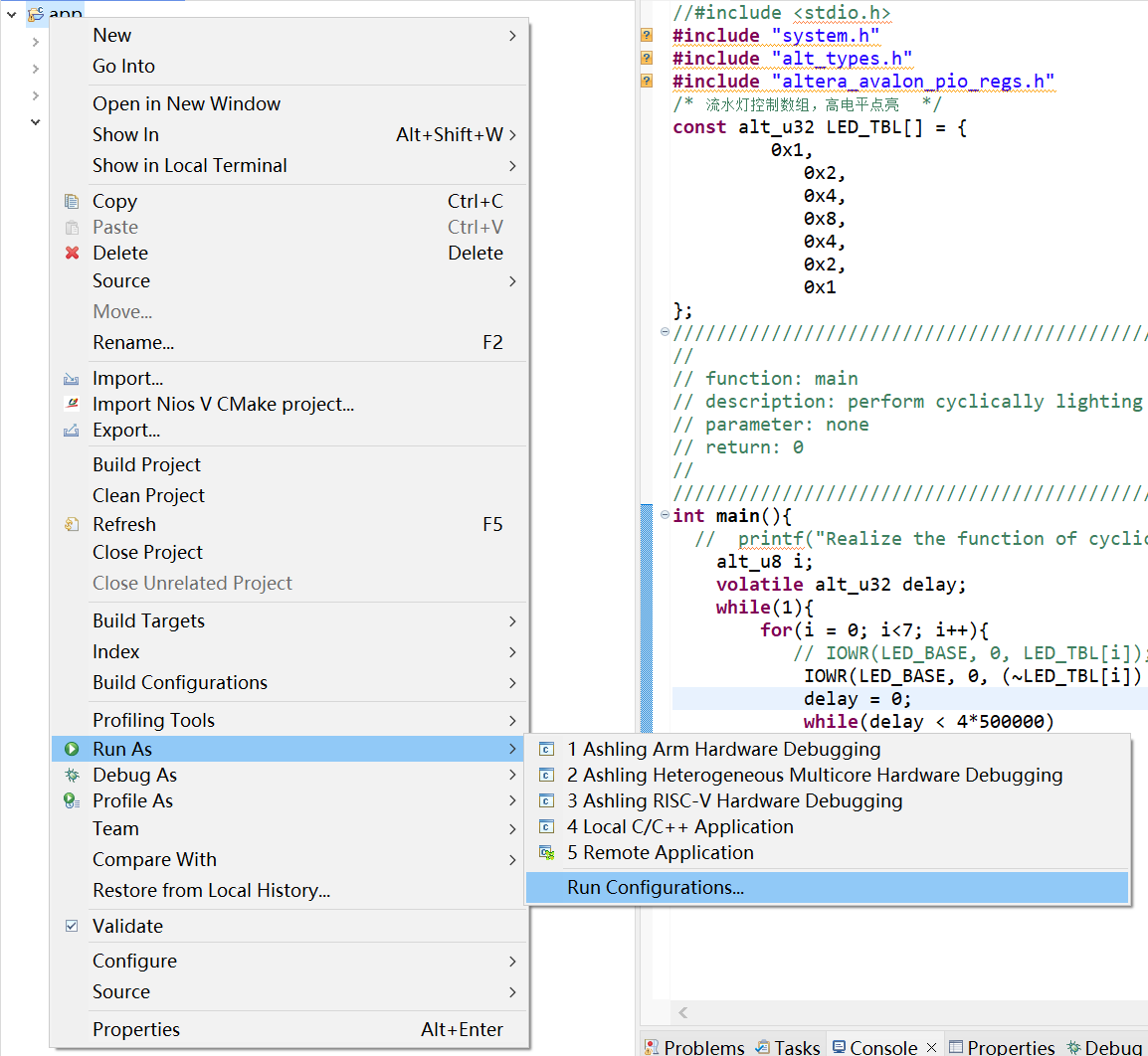
选择RISC-V 的启动选项:Debugger -> Auto-Detect Scan Chain。固件下载后应该能找到Nios V Core。点Apply 再run。
如果要JTAG-UART终端:在Nios V Command Shell里运行juart-terminal。(本次因ram太小,放不下printf 所以不做相关测试。)
2. Quartus 25.1 Standard 综合 Nios V 时出现 riscv.pkg.sv 错误
2.1 遇到的错误
曾出现类似:
Error (10835): SystemVerilog error at riscv.pkg.sv(...): no support for unions
Error (10355): SystemVerilog Enumeration Type Declaration error ...
包括:
no support for unions
encoded value ... does not match the width of the enumeration's base type
2.2 原因
不要把 Nios V Platform Designer 的 .qsys 系统直接当成普通 HDL 源去综合。
正确流程是:
Platform Designer .qsys
        ↓
Generate HDL
        ↓
生成 synthesis/ 下的 HDL + .qip
        ↓
Quartus 工程加入生成的 .qip
2.3 解决
- 在 Platform Designer 中 Generate HDL。
- 从 Quartus 工程中去掉错误加入的
.qsys/QSYS_FILE。 - 加入生成目录里的
.qip/QIP_FILE。 - 删除旧增量数据库后重新综合:
db/ incremental_db/ - 不要去手改
riscv.pkg.sv。
3. .qip 到底怎么在顶层实例化
.qip 是 Quartus 的 IP 文件集合描述,不是 Verilog module。
应该实例化 Platform Designer 生成 HDL 中的顶层模块,比如系统名叫:
niosv
则类似:
niosv u0 (
    .clk_clk                         (clk),
    .reset_reset_n                   (reset_n),
    .led_external_connection_export (led)
);
实际端口名以生成文件为准。
可以看:
niosv/synthesis/niosv.v
或者 Platform Designer 生成的:
niosv_inst.v
模板。
4. 怎么确认 LED PIO 真的是 4 bit
Platform Designer 中将 LED PIO 设置成 Width = 4 后,最直接的确认方式不是“凭记忆”,而是看生成 HDL。
例如在:
niosv/synthesis/niosv.v
搜索:
led_external_connection_export
如果看到:
output wire [3:0] led_external_connection_export;
就明确说明:
[3:0] = 4 bit
顶层也应该对应:
wire [3:0] led;
最终实际检查的 Platform Designer PIO 参数也确实为:
LED
Direction = Output
Width = 4
5. 从 128 KB On-Chip RAM 改成 32 KB
5.1 32 KB 地址范围
32 KB = 32768 Byte = 0x8000 Byte
从 0x00000000 起:
0x00000000 ~ 0x00007FFF
因此原 CMakeLists 中:
COMMAND elf2hex app.elf -o RAM.hex -b 0x00000000 -w 32 -e 0x00007FFF -r 4
实际上已经是 32 KB 配置。
如果是 128 KB,应是:
128 KB = 0x20000 Byte
结束地址 = 0x0001FFFF
5.2 不能只改 elf2hex
elf2hex 是在 ELF 已经成功链接后执行的。
真正决定 .text/.rodata/.rwdata/.bss/heap/stack 可以放在哪里的是 BSP 生成的 linker script:
-T "${BspLinkerScript}"
因此正确流程:
Platform Designer 把 RAM 改成 32 KB
        ↓
Generate HDL / 更新 .sopcinfo
        ↓
更新 BSP
        ↓
BSP linker memory = 32 KB
        ↓
重新编译 app.elf
        ↓
elf2hex 生成 0x0000~0x7FFF 的 RAM.hex
6. .rwdata/.bss is not within region RAM
6.1 第一轮错误
出现:
address 0x8494 of app.elf section `.rwdata' is not within region `RAM'
address 0x9fec of app.elf section `.bss' is not within region `RAM'
32 KB RAM 的末端只有:
0x7FFF
因此 .rwdata、.bss 已经超界。
这说明:
linker script 的 32 KB RAM 限制已经生效,但程序太大。
不是 elf2hex 的问题,因为此时 app.elf 都还没成功生成。
7. printf 对小 RAM Nios V 的影响
原 LED 程序包含:
#include <stdio.h>

printf("Realize the function of cyclically lighting the LED\n");
对于这种只有 32 KB RAM 的裸机程序,printf/newlib 会明显增加体积。
注释掉:
#include <stdio.h>
printf(...);
之后,错误缩小到:
address 0x8fec of app.elf section `.bss' is not within region `RAM'
也就是确实减小了一部分,但仍然没完全解决。
因此本次结论:
printf是体积因素之一,但不是最终根因。
8. 真正解决 32 KB 链接失败:Release 构建
检查 settings.bsp 发现:
hal.make.cflags_debug
Value = -g
而 Release 才会使用:
hal.make.cflags_optimization
Value = -O2
RiscFree / CMake 工程默认使用 Debug,因此 BSP 的 -O2 没有实际启用。
8.1 命令行正确的 Release 构建
推荐:
cmake -S software/app ^
      -B software/app/build/Release ^
      -G "Unix Makefiles" ^
      -DCMAKE_BUILD_TYPE=Release
然后:
cmake --build software/app/build/Release
如果旧 build tree 已经缓存 Debug,先删:
rmdir /s /q software\app\build
再重新配置。
8.2 也可以让 CMake 默认 Release
在 project(app) 前加:
if(NOT CMAKE_BUILD_TYPE)
    set(CMAKE_BUILD_TYPE Release CACHE STRING "Build type" FORCE)
endif()
注意:如果 IDE 显式传入 -DCMAKE_BUILD_TYPE=Debug,这个条件不会覆盖它。
9. 成功生成 ELF 和 RAM.hex
最终构建输出:
[ 94%] Built target hal2_bsp
[ 96%] Linking C executable app.elf
[ 96%] Built target app.elf
[ 97%] Creating app.elf.objdump.
[ 98%] Reporting memory available for stack + heap in app.elf.

app.elf

- 24.91 KB - Program size (code + initialized data).
- 1260 B - Free for stack + heap.

[100%] Creating RAM.hex.
[100%] Built target create-hex
这说明软件构建链完整成功:
led.c
 ↓
.o
 ↓
app.elf
 ↓
objdump
 ↓
stack report
 ↓
RAM.hex
为什么 24.91 KB 后只剩 1260 B?
因为:
Program size (code + initialized data)
并不等于全部 RAM 占用。
.bss 同样需要占 RAM,但并不属于 ELF 中的“初始化数据文件大小”。
因此实际大概是:
.text + .rodata + initialized data
+ .bss
+ stack/heap remaining
= 32 KB
最终只剩:
1260 B
给 stack + heap。
对于当前简单 LED 程序够用,但以后加入:
printfmalloc- 大局部数组
- 更多驱动
- C++
- 较深函数调用
就需要重新关注 RAM。
10. 如果以后还想进一步缩小 BSP
本次 Release 已经能跑,因此以下属于可选优化,不是本次必须操作。
settings.bsp 中曾确认这些选项默认并不“极致省空间”:
hal.linker.use_picolibc = 0
hal.enable_exit = 1
hal.enable_clean_exit = 1
hal.enable_c_plus_plus = 1
hal.enable_reduced_device_drivers = false
hal.enable_lightweight_device_driver_api = false
可选方向:
-Os
-ffunction-sections
-fdata-sections
-Wl,--gc-sections
以及:
hal.enable_reduced_device_drivers = true
hal.enable_lightweight_device_driver_api = true
hal.enable_c_plus_plus = false
hal.enable_exit = false
hal.enable_clean_exit = false
最后还可考虑:
hal.linker.use_picolibc = true
但要根据工程需求决定,不要为了省几个 KB 无脑全开。
11. 命令行创建 BSP / App
本次使用的 CLI flow:
niosv-bsp -c -t=hal --sopcinfo=niosv.sopcinfo software/bsp/settings.bsp
创建 application:
niosv-app -a=software/app -b=software/bsp -s=software/app/led.c
其中:
software/bsp/settings.bsp
就是 BSP 的核心配置文件。
这套流程不依赖 BSP Editor GUI。
12. 硬件逻辑改完后,软件怎么重新适配
硬件修改后:
Platform Designer
→ Generate HDL
→ 生成新的 .sopcinfo
→ Quartus Full Compilation
→ 新 .sof
如果 settings.bsp 仍然关联同一个 niosv.sopcinfo,更新已有 BSP:
niosv-bsp -u software/bsp/settings.bsp
错误写法
曾尝试:
niosv-bsp -u --sopcinfo=niosv.sopcinfo software/bsp/settings.bsp
报:
SOPCINFO file can not be changed via update.
Please create a new BSP with the SOPCINFO file.
原因是 -u 不能拿来切换 SOPCINFO 文件。
settings.bsp 本身已经记录:
..\..\niosv.sopcinfo
所以直接:
niosv-bsp -u software/bsp/settings.bsp
即可。
一般不需要重新 niosv-app
niosv-app 是创建 application 骨架。
硬件地址变化主要靠:
.sopcinfo → BSP → system.h/linker script
更新。
13. RiscFree 报 no harts found
初始错误:
Error in GDB server launch sequence

Ashling GDB Server for RISC-V
Initializing connection ...
Error occurred during enumeration of RISC-V harts (no harts found).
最开始还伴随 USB-Blaster I:
Cannot set the JTAG frequency
Failed to get JTAG frequency from the debug probe
当时曾怀疑下载器。
但后续实验非常关键。
14. jtagconfig -d 已经能看到 Nios V
USB-Blaster I 时:
1. USB-Blaster [USB-0]
   020F20DD  10CL016(Y|Z)/EP3C16/EP4CE15
   - Node ... JTAG UART #0
   - Node ... Nios V #0
后来 FT4232H 改 USB-Blaster III 后仍能看到:
1. USB <-> Serial Converter [USB-1]
   020F20DD  10CL016(Y|Z)/EP3C16/EP4CE15
   - Node 0C006E00  JTAG UART #0
   - Node 08986E00  Nios V #0

JTAG clock speed 5 MHz
说明:
PC → JTAG probe → FPGA TAP → SLD → Nios V JTAG node
已经能通。
但:
jtagconfig看见Nios V #0只说明 Debug Transport/JTAG 节点存在,不保证 CPU hart 能正确进入 Debug Mode。
15. 用 niosv-download 排除 IDE GUI 问题
测试:
niosv-download software/app/build/Release/app.elf --go
当时输出:
ash-riscv-gdb-server
--auto-detect true
--probe-type usb-blaster-2
--instance 1
--device 020F20DD
--core-number 0
最后仍:
Error occurred during enumeration of RISC-V harts (no harts found).
这说明:
问题不是单纯 RiscFree IDE GUI 的 Run Configuration。
16. USB-Blaster III 实验说明了什么
后来用 FT4232H 做了 USB-Blaster III 实验:
quartus_pgm -l
能看到:
USB <-> Serial Converter [USB-1]
而:
ash-riscv-gdb-server --list-probes
输出:
Cable Index  Persistent ID  Type           Display Name
1            1              USB-Blaster-2  USB <-> Serial Converter [USB-1]
说明 Ashling 已经能识别这个 probe。
但它仍然:
no harts found
最终结论
因此本次 no harts found 不能归咎于 USB-Blaster。
USB-Blaster III 的制作和测试单独记录在:
FT4232H_USB_Blaster_III_制作记录.md
17. 最终根因:Platform Designer Debug Reset 接错
看 Platform Designer 连接图后发现:
My_NiosV.ndm_reset_in
被接到了普通 system reset 网络;
而:
My_NiosV.dbg_reset_out
没有正确接回去。
这是 Debug Reset 网络错误。
17.1 正确连接
普通系统复位:
clk_0.clk_reset
    ├── My_NiosV.reset
    ├── RAM.reset1
    ├── DEBUG.reset
    └── LED.reset
Debug Module Reset:
My_NiosV.dbg_reset_out
          │
          └── My_NiosV.ndm_reset_in
核心原则:
dbg_reset_out → ndm_reset_in
不要:
dbg_reset_out → My_NiosV.reset
也不要把:
ndm_reset_in
当普通 reset 使用。
修正后重新:
Generate HDL
→ Quartus Full Compile
→ 更新 BSP
→ Build Release
→ 下载 .sof
→ niosv-download / RiscFree
最终跑通。
18. dm_agent 也必须这样连
为了 RISC-V Debug Module 正常工作:
Nios V instruction_manager
    ├── RAM
    └── dm_agent

Nios V data_manager
    ├── RAM
    ├── LED
    ├── DEBUG / JTAG UART
    ├── timer_sw_agent
    └── dm_agent
本次 dm_agent 地址:
0x00020000
需要保证:
instruction_manager → dm_agent = 0x00020000
data_manager        → dm_agent = 0x00020000
两边一致。
Nios V 的 debug 实现需要 CPU halt 后跳进 Debug Module 的 park loop,因此 instruction/data bus 都能访问 dm_agent 很重要。
19. 顶层没有外部 reset 引脚是不是一定错
不是。
要区分:
“没有板级 Reset 按键”
和:
“Nios V reset 根本没有合理驱动”
Platform Designer 可以通过 Reset Bridge / Reset Release 等方式在内部构造 reset 网络,不一定要导出物理 reset 引脚。
但必须保证:
My_NiosV.reset
RAM.reset1
JTAG UART.reset
PIO.reset
得到正确 reset。
对于 Debug Module,如果启用了:
Enable Reset from Debug Module
则额外保证:
dbg_reset_out → ndm_reset_in
20. RiscFree 中怎样用 Release
RiscFree 的 Nios V CMake 工程默认很容易落到 Debug。
关键不是传统 Eclipse 的 “Debug/Release configuration” 下拉框,而是:
CMAKE_BUILD_TYPE
如果 IDE 里能设置 CMake arguments:
-DCMAKE_BUILD_TYPE=Release
即可。
若 GUI 不明显,命令行构建最可靠:
cmake -S software/app ^
      -B software/app/build/Release ^
      -G "Unix Makefiles" ^
      -DCMAKE_BUILD_TYPE=Release

cmake --build software/app/build/Release
检查实际编译命令中是否出现:
-O2
21. RiscFree 点 Build Project 没看到编译输出
这是 Console 视图的问题,不是没编译。
打开:
Window
→ Show View
→ Console
若菜单没有:
Window
→ Show View
→ Other...
→ General
→ Console
Console 右上角使用:
Display Selected Console
切换到:
CMake Console
Make / CDT Build Console
而不是:
Ashling GDB Server
GDB Console
如果工程没有变化,增量构建可能几乎没输出。
可以:
Project → Clean
后再 Build。
22. Debug session 'app.elf' is already running
重新修改程序后再次 Run/Debug,RiscFree 曾报:
Debug session 'app.elf' is already running or not terminated completely.
原因是上一次:
Ashling GDB Server / GDB Debug Session
仍在运行或没有彻底退出。
解决:
- 打开 Debug View。
- 选中旧
app.elfsession。 - 点击红色方块:
Terminate - Console 中若仍有 Ashling GDB Server,也 Terminate。
- 再 Run / Debug。
- 若 IDE 状态没清干净,重启 RiscFree。
- 极端情况可在任务管理器结束:
ash-riscv-gdb-server.exe
riscv32-unknown-elf-gdb.exe
23. LED 低电平点亮怎么改
原高电平点亮表:
const alt_u32 LED_TBL[] = {
    0x1,
    0x2,
    0x4,
    0x8,
    0x4,
    0x2,
    0x1
};
如果 4 个 LED 是:
0 = 亮
1 = 灭
可直接写:
const alt_u32 LED_TBL[] = {
    0xE,
    0xD,
    0xB,
    0x7,
    0xB,
    0xD,
    0xE
};
更推荐保留“1 代表想点亮哪个 LED”的逻辑表,然后输出时统一反相:
IOWR(LED_BASE, 0, (~LED_TBL[i]) & 0xF);
例如:
~0x1 & 0xF = 0xE
~0x2 & 0xF = 0xD
~0x4 & 0xF = 0xB
~0x8 & 0xF = 0x7
最终代码:
#include "system.h"
#include "alt_types.h"
#include "altera_avalon_pio_regs.h"

const alt_u32 LED_TBL[] = {
    0x1,
    0x2,
    0x4,
    0x8,
    0x4,
    0x2,
    0x1
};

int main(void)
{
    alt_u8 i;
    volatile alt_u32 delay;

    while (1) {
        for (i = 0; i < 7; i++) {
            IOWR(LED_BASE, 0, (~LED_TBL[i]) & 0xF);

            delay = 0;
            while (delay < 500000)
                delay++;
        }
    }

    return 0;
}
delay 使用:
volatile
是为了防止 Release 优化时编译器把纯延时循环直接消掉。
24. 最终推荐的一套完整工作流
24.1 第一次建立硬件
Quartus project
   ↓
Platform Designer
   ↓
Nios V + RAM + JTAG UART + PIO
   ↓
正确连接 clock/reset
   ↓
instruction_manager/data_manager → dm_agent
   ↓
dbg_reset_out → ndm_reset_in
   ↓
Assign Base Addresses
   ↓
Generate HDL
   ↓
Quartus 加生成 .qip
   ↓
Full Compilation
24.2 创建 BSP
niosv-bsp -c -t=hal --sopcinfo=niosv.sopcinfo software/bsp/settings.bsp
24.3 创建 App
niosv-app -a=software/app -b=software/bsp -s=software/app/led.c
24.4 Release Build
cmake -S software/app ^
      -B software/app/build/Release ^
      -G "Unix Makefiles" ^
      -DCMAKE_BUILD_TYPE=Release

cmake --build software/app/build/Release
目标看到:
Built target app.elf
Creating RAM.hex
Built target create-hex
24.5 下载 FPGA
Quartus Programmer 下载最新:
.sof
24.6 检查 JTAG
jtagconfig -d
应至少看到:
JTAG UART #0
Nios V #0
24.7 下载软件
niosv-download software/app/build/Release/app.elf --go
或者从 RiscFree Run / Debug。
25. 硬件改动后的最短更新流程
Platform Designer 修改
        ↓
Generate HDL
        ↓
Quartus Full Compile
        ↓
niosv-bsp -u software/bsp/settings.bsp
        ↓
重新 CMake Release Build
        ↓
下载新 .sof
        ↓
下载新 app.elf
如果只改 led.c,无需重新 Platform Designer / BSP:
改 led.c
→ Build Project
→ Terminate 老 Debug session
→ Run / Debug
26. 本次排错最重要的经验
26.1 不要看到 no harts found 就立刻怪下载器
本次非常典型:
USB-Blaster I → no harts found
FT4232H / USB-Blaster III → 仍然 no harts found
后续检查才发现是:
Platform Designer Debug Reset 接错
因此推荐排查顺序:
1. jtagconfig -d 是否看到 FPGA
2. 是否看到 Nios V #0
3. CPU clock 是否正常
4. 普通 reset 是否正常
5. instruction/data manager 是否都连 dm_agent
6. dm_agent 两边 base address 是否相同
7. dbg_reset_out 是否正确连 ndm_reset_in
8. 再考虑 probe / IDE / driver
26.2 编译问题和下载/调试问题分开
编译阶段:
C/C++ → ELF → RAM.hex

FPGA 阶段:
Platform Designer → QIP → SOF

调试阶段:
Probe → JTAG → Debug Module → hart
不要把三个层面混在一起排查。
27. 两个常用诊断命令
看 Quartus/JTAG Server:
jtagconfig -d
看 Ashling 自己识别到的 Probe:
ash-riscv-gdb-server --list-probes
看 Quartus 编程线:
quartus_pgm -l
跳过 IDE,直接下载 ELF:
niosv-download software/app/build/Release/app.elf --go
这四个命令非常适合逐层定位。
28. 参考资料
本记录主要依据本次实际排错过程整理。
用户提供的两个 ChatGPT 分享链接:
- https://chatgpt.com/share/6a770b39-ef70-83ec-9e3b-0613d30971e6
- https://chatgpt.com/share/6a770b0a-0954-83ec-8170-91df41b63457
Altera 官方资料:
- Nios V Processor Reference Manual — Reset and Debug Signalshttps://docs.altera.com/r/docs/683632/25.3.1/nios-v-processor-reference-manual/reset-and-debug-signals
- Nios V Embedded Processor Design Handbook — Debug Tabhttps://docs.altera.com/r/docs/726952/26.1/nios-v-embedded-processor-design-handbook/debug-tab
- Enabling RISC-V based Debug Modulehttps://docs.altera.com/r/docs/726952/26.1/nios-v-embedded-processor-design-handbook/enabling-risc-v-based-debug-module
- Nios V Tutorial — Creating a Platform Designer System
https://docs.altera.com/r/docs/784468/current/an-985-nios-v-processor-tutorial/creating-a-platform-designer-system
附:这次最后真正解决问题的一句话
32 KB 软件放不下:用 Release;RiscFree
no harts found:最终修正 Platform Designer 的dbg_reset_out -> ndm_reset_inDebug Reset 连接。